CMOS sensor technique enters the super-high resolution area up to 150 MP. This opens new opportunities to skip CCD with more quality, speed, better prices and faster developement.
CMOS image sensor technology has turned into the new normal. Well, not entirely… For high-end resolutions above 30 Megapixels, users still require CCD imagers to acquire high-resolution images. But now, CMOS sensors are available with high and super-high resolution, and bring numerous benefits for developers of demanding applications in terms of quality, speed, pricing, and time-to-market.
Sony’s decision to execute their CCD end-of-line (EOL) opened the way to a secure CMOS transition in all areas, with reliable ten-years transition plans. This evolution has boosted CMOS development since then and changed the whole vision industry. Progressively over the years the quality of CMOS has steadily increased over all sensor criteria, enabling them to become a complete CCD replacement. It was only for resolutions of 50 Megapixel or above, that there was virtually no available CMOS equivalent, until now. Vision engineers developing super high-resolution applications can now take advantage of CMOS benefits in both implementation and performance.
The New Ultra-Performing CMOS Image Sensors
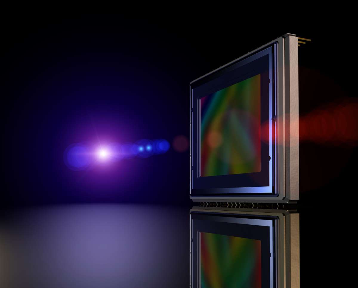
The recently released SONY high-resolution sensor line up, shown in Figure 1, provides up to 150 Megapixel resolution. With pixel pitches of 3,76µm and 4.6µm, frame rates of 6 fps@14bit can be achieved at full resolution, up to 30 fps are possible at 4K. The high-resolution image sensors use microfabrication technologies to improve picture quality, come with a High Dynamic Range function (HDR) and provide rich graduation expression based on a high-res AD converter with up to 16bit. Compared to CCD imagers, these mega-imagers provide great image uniformity, which is crucial for high-end inspection tasks; an application where CCD’s had a plus in the past.

Figure 1: Matrix of Image Size and Resolution for SONY’s high-resolution imagers
The IMX161 and the IMX211 come with 8-lanes LVDS output, while the other high-resolution sensors provide Sony’s latest interface innovation SLVS-EC for transferring the highest amount of captured data at high-speeds; the maximum output is 18.4 Gbps on 8 lanes, or 2.3Gbps per channel. The SLVS-EC (Scalable Low Voltage Signaling – Embedded Clock) diverges from most contemporary interfaces by embedding the clock within the data line. This serial transmission is received by hardware; that is, an ASIC, FPGA, or similar device, which recovers the clock from the signal and then uses the clock with the original data stream to correctly sample it. This feature leads to better timing, and, connected to an FPGA, it enables on-board processing for intelligent vision.
|
|
IMX211 |
IMX411 |
IMX461 |
| Image Size |
Type 4.2 (66.7mm) |
Type 4.2 (66.7mm) |
Type 3.4 (55mm) |
| Number of Pixels |
100M pixels |
150M pixels |
100M pixels |
| Pixel Size |
4.6 µm |
3.76 µm |
3.76 µm |
| Frame Rate |
All-pixels/2.0fps@14bit |
All-pixels/4.0fps@14bit |
All-pixels/6.0fps@14bit |
| Output |
LVDS |
SLVS-EC |
SLVS-EC |
Figure 2: Characteristics of the SONY high-resolution sensors
These mega imagers are perfect fit for high-end applications in ITS, traffic surveillance, and robotic control. In addition, they are suitable for very precise industrial inspection for quality checking displays, digital archives and aerial imaging. This superior detailed imaging results in both time and resource savings for all inspection tasks. This kind of performance from high-end CMOS devices will not only reduces costs, but will increase safety, too, with their increased quality for inspections.
CMOS Implementation Saves Time and Effort
Taking advantage of the new high-resolution imagers, engineers who have dealt with high-res CCD sensors in the past, can now take advantage of the general CMOS benefits to improve their product development. The implementation of CMOS image sensors requires less time and is less complicated compared to CCD sensors. The technical structure of CCD and CMOS imagers differ radically. A CMOS imager is an all-in-one product, equipped with an A/D converter, correlated double sampling, digital interfaces and the sensor control; together on a single chip. In the CCD world, all these entities are single components and must be merged by the engineer. Therefore, CCD imaging needs dedicated knowledge, time, and an analog skill set. CMOS implementation is faster and easier; almost every technically trained engineer is capable of building a CMOS camera. This facility reduces the development cycles and the time-to-market for CMOS based devices; in digital times with shortened product and development spans – let’s face it – they are a CCD killer. Technological trends helped to accelerate the success of CMOS imagers. The smaller pixel pitches of CMOS imagers enable miniaturized designs. This fact drives embedded vision solutions in all industrial and consumer applications. In addition, CMOS sensors score with particularly favourable pricing; cheaper lenses; and, accessories as a bonus. Normally, one could now say, “What is the drawback here?”. But there isn’t any. CMOS image sensors arrive with tremendous image quality improvements at the same time.
Imaging Performance without a Snag
Performance is the key CMOS feature, especially with the new mega imagers and their high-end resolution. The initial decisive step in the evolution of CMOS sensors was the acquisition of images with global shutter pixel control technology and combining this advance with vastly increased speed and outstanding image quality. Moving objects can be captured simultaneously, without artifacts and with increased sharpness. In addition, their architecture and parallel pixel readout makes CMOS sensors many times faster their conventional CCD equivalents. CMOS technology permits very high frame rates and defines the maximum of todays speed.
The improvements in manufacturing processes enable a much-improved ratio between sensor size, active pixel area (fill factor), and implicitly, the maximum utilization of incident light. Therefore, together with other factors, CMOS sensors provide high resolution, high sensitivity, quantum efficiency, high dynamic range, and very low noise. In fact, now CMOS sensors can be used in low-light applications to produce very good image quality. In addition, CMOS sensors offer a wider range of functions; lower energy consumption; and, are more flexible for industrial applications. Overall, CMOS imagers achieve better results than CCD sensors, even in demanding applications.
Additionally, to these many advantages, and for applications in need of high resolution, vision engineers had to make extra effort for the implementation of CCD sensors and accept their limitations. Now, CMOS sensors have overtaken all aspects of CCD technology and comes with many advantages in addition, boosting vision performance extremely and influencing the further development of the whole vision industry.
Tools and Support for Successful CMOS Implementation
The modern CMOS sensors with their vastly improved image quality, maximized speed and expanded functionalities have developed into the fundamental digital component of any (embedded) vision system, and now for high-resolutions, as shown with the new mega imager line up above. The integrated circuits can be relatively easily designed and implemented. However, the application challenge lies in achieving the best-possible image quality with the given devices and component settings – especially, when it comes to using the high-resolution for achieving the best possible results. Evaluation boards and Reference Design Kits (RDKs) help the designer to select the correct sensor and utilize its full functionality with its detail settings. RDKs including Gerber files; sensor boards with prefabricated designs; and, finished IP blocks allow direct development on the sensor, and verify its suitability for the desired application and the required image quality.
There are more tools to avoid standard errors: Therefore, to shorten development cycles and achieve faster implementation and time-to-market, ready-to-go IP packages like the FRAMOSÒ SLVS-EC IP Core can connect the SLVS-EC imager with Xilinx FPGAs and SoCs. Manufacturers or OEMs whose core competence does not lie in image processing or camera technology can retain their original focus with the assistance of external experts, and still implement mature imaging solutions with the SONY high-resolution line up in their devices.