How Embedded Vision Developers Can Achieve High-Speed Sensor Interfacing and Easy Design-Ins.
A ready-to-integrate processing block for Sony’s 3rd generation CMOS Global Shutter image sensors equipped with the SLVS-EC interface accelerates the time-to-market and improves performance for vision development on XILINX FPGAs.
Sony’s SLVS-EC interface standard has emerged as the high-speed interface to Sony’s latest image sensors, enabling higher throughput, greater signal integrity, and simpler designs. Engineers that develop solutions with the Xilinx FPGAs and SoCs can take advantage of FRAMOS®’s SLVS-EC RX IP Core, Evaluation Board, and pre-tested source code examples. Device builders and camera vendors can reduce design risks and decrease the time-to-market, while reaping the benefits of Sony’s latest high-speed interface.

The innovations of Sony’s 3rd generation Pregius image sensors elevate vision applications to new heights by boosting the speed of the image data transfer without sacrificing image quality. The SLVS-EC interface (Scalable Low-Voltage Signaling with Embedded Clock) with up to 8 lanes and 2.376 Gbps throughput per lane, satisfies ever more demanding industry requirements, for both high resolution and high speed. When compared to Sony’s second-generation CMOS image sensors with S-LVDS interfaces, the SLVS-EC interface doubles the overall output speed to 19 Gbps. SLVS-EC has more than three times higher bandwidth per lane. As such, SLVS-EC will enable new high-performance image sensors with higher resolution while allowing simplified system designs.
SLVS-EC sets a new standard for high-speed interfaces for image sensors. The SLVS-EC interface allows users to deploy faster sensors with increased performance and longer cable lengths. In addition, it permits a simplified and smaller hardware design by requiring fewer lanes for the same bandwidth. The robust embedded clock in the interface prevents clock skew, to allow higher throughput while making dedicated clock lanes obsolete. Just the same, implementation of this interface brings challenges to OEMs, device builders, and vision engineers.
The Benefits and Challenges for Vision System Designers
Embedded Vision derives a huge potential from embedded processing and intelligent algorithms that drive autonomous devices as independent decision makers. Many autonomous smart devices such as robotic vacuums or lawn mowers, could not exist without a fast and powerful on-board processing system that includes a Field Programmable Gate Array (FPGA). FPGAs, in many vision systems, manage sensor control and timing; perform image pre-processing, and transfer data to common interfaces. For example, FPGA blocks and Systems-on-Chip (SoC) for device builders are scalable industrial IoT platforms from edge-to-cloud. In addition, product builders are empowered with intelligent and adaptive assets to connect from silicon to solution. The FPGA approach enables compact and capable machine vision. This embedded solution drives integration levels; intelligence; maximizes performance; and, power trends that will maximize capabilities. At the same time, it minimizes power consumption and the hardware footprint.
Vision developers and OEM’s who purchase fast sensors on one hand, and view FPGAs as intelligent assets on the other, must link these two building blocks. The rapid development of FPGA-based vision solutions requires both specialized knowledge and developers with experience in the integration of new imagers. Additionally, the more complex SLVS-EC interface will require more development effort and overhead for general sensor implementation throughout the necessary byte-to-pixel conversion, and the correct transceiver configuration. Conversely, most vision engineers desire to be more efficient; maintain focus on their core specialization, or their “killer” application while keeping development cycles short. Of course, the right development tools and SDKs to help vision engineers achieve these goals.
How Dedicated IP Cores Connect Sensors to an FPGA
Specific IP cores perform signal conversion within the FPGA or SoC, by receiving the sensor data using an easy and well documented interface. This configuration reduces time-to-market by providing a pre-designed logic block. The FRAMOS developed SLVS-EC RX IP Core for Xilinx FPGAs and SoCs provides a trusted, familiar implementation of the SLVS-EC and is Sony’s preferred interface for advanced image sensors. The SLVS-EC IP Core connectivity between the sensor and FPGA is shown in Figure 1:

Figure 1: How the SLVS-EC IP Core facilitates connection between sensor and FPGA
The IP Core is an on-chip function block that connects the FPGA logic with the image sensor’s data stream; it receives the interface data and manages the byte-to-pixel conversion for various lane configurations. This process prepares a highly-efficient processing workflow to be run by the FPGA. The software supports SLVS-EC v1.2 with 1, 2, 4, and 8 lanes that are configurable by the user. In addition, it delivers 8 to 14-bit pixel formats of raw data. The IP core supports dynamic mode changes and contains an AXI4 communication and control interface. Minimizing the risks in sensor implementation significantly accelerates the development of a sensor and FPGA solution:
Dr. Simon Che’Rose, Head of Development at FRAMOS sees many advantages for system designers: “Each customer using SONY image sensors, either working with high-speed or embedded solutions, will benefit from the SLVS-EC interface and its unique features. The RX IP Core Block for Xilinx FPGAs, in combination with the full documented evaluation kit, makes integration and system development easy, resulting in a faster time-to-market for customer applications working with the SLVS-EC.”
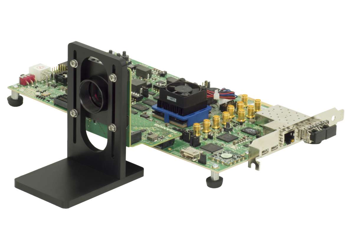
It is crucial to get up to speed in the development and integration of sensors and FPGAs in these times of rapid digitization. In addition, it is important to deal with the volatile and fast-growing businesses and markets in vision technology. Ready-to-implement IP cores are available as extended packages to support vision engineers in meeting their goals. These IP cores include design files, simulation environments (e.g., ModelSim) and, dedicated reference implementation examples. An evaluation board (EVB) is available to provide examples and designs that guide the development, implementation, and testing of an SLVS-EC based sensor. This package includes the hardware and software environment and documented implementation examples with source code. This development kit provides a complete foundation for the image sensor to incorporate an SLVS-EC RX IP Core. An example of a camera and sensor evaluation extension package for the Xilinx UltraScale Evaluation Board is shown in Figure 2:

Figure 2: Camera design testing using a sensor evaluation extension package for Xilinx UltraScale+ Evaluation Boards
Maximizing Innovation by Purchasing a Pre-Designed Expert Solution
State-of-the-art IP Cores combine the most successful and reliable sensors and FPGAs to build high-resolution and high-speed applications, with on-board intelligence. Machine builders, OEMs, and camera manufacturers in both the Embedded Vision and classic Machine Vision segments benefit from a seamless upgrade to new technology and higher performing solutions, maximizing their innovative strengths. Implementation of the SLVS-EC RX IP Core for embedded vision development helps to avoid resource or capacity issues, and increases planning efficiency. This embedded solution meets the requirements for development time, performance and cost targets, and offers a practical solution for the technical challenges that face developers.