By Christopher Ivey
As a marketing content creator for FRAMOS, I sometimes struggle with understanding the more technical aspects of our products and services. To help remedy this and to learn more about our new Time-of-Flight camera development kit, I reached out to Chris Baldwin – a senior application engineer with FRAMOS. Chris has been deeply involved with the development of new Time-of-Flight products for the company and was the perfect individual to help introduce me to our development kit. I also wanted to discuss some of the customization possibilities for the kit.
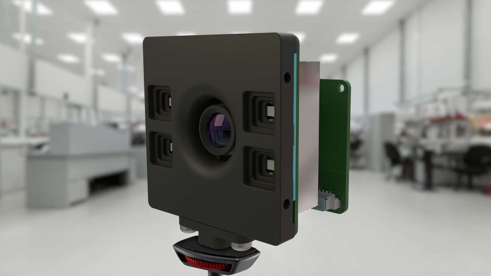
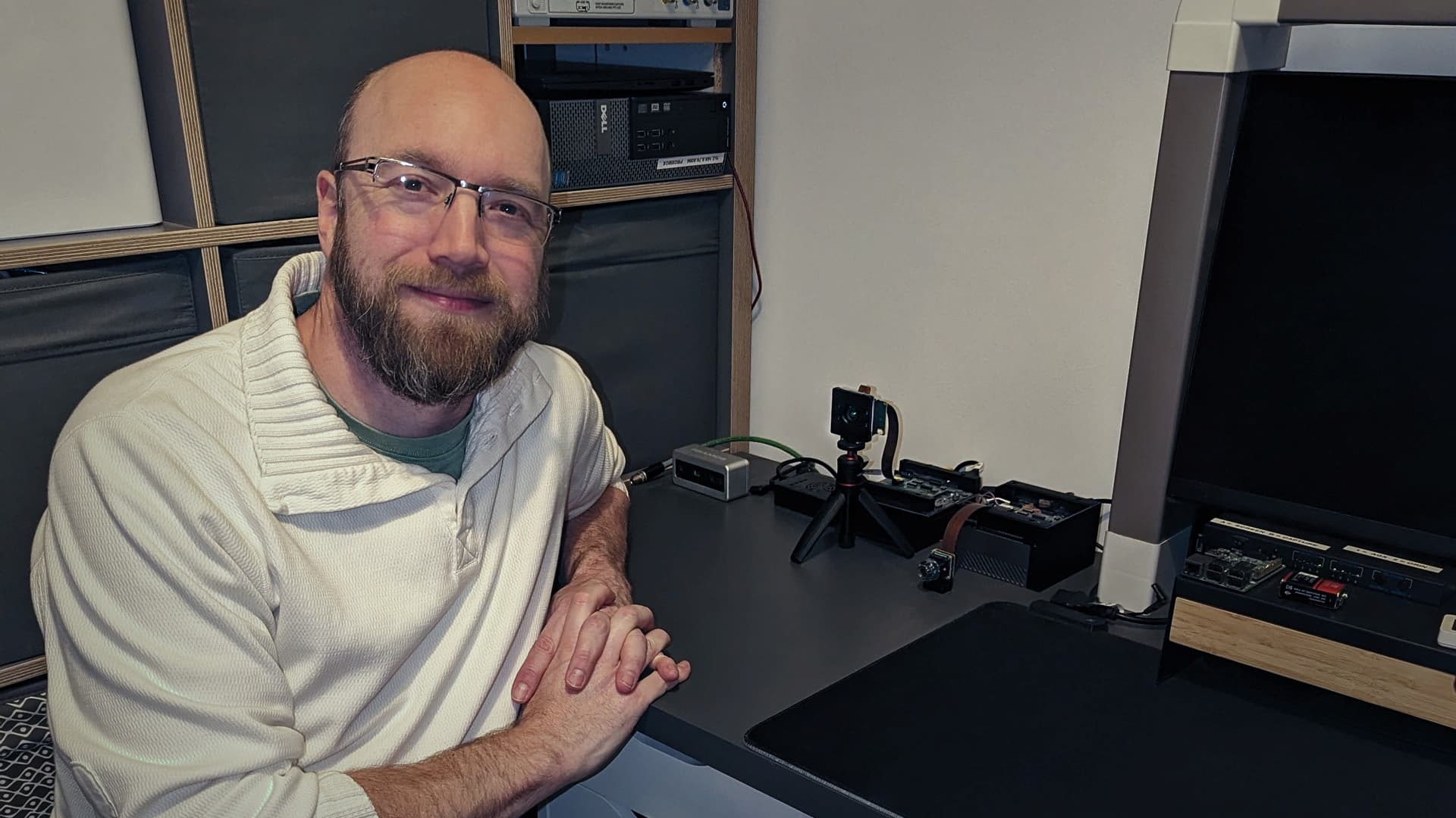
Since we happen to live and work on opposite sides of the Atlantic Ocean, I ended up talking with Chris over videoconference. He joined me from his home workshop – a surprisingly neat space crowded with oscilloscopes, a bewildering variety of computing devices, and a large collection of camera modules of different shapes and sizes. The development kit we had agreed to talk about had pride of place: a neat little cube fronted with a lens surrounded by laser emitters, poised on a tiny tripod.
After some informal introductions I got down to the business of talking about Time-of-Flight Technology and the FSM-IMX570 development kit in particular.
Just as an introduction, Chris, can you tell us a little about yourself and what you do at FRAMOS?
Hi Chris, great name by the way. Yes, I am a member of the FRAMOS Technical Solutions and Support team as an Imaging Expert. I have been in the Vision industry for over 20 years with the last 11 years being with FRAMOS. My day-to-day work is helping customers determine the most appropriate imaging technology for their product as well as getting those systems up and running in the prototype, through to the production implementations.
We’re going to be talking about what FRAMOS can do to customize their new ToF development kit for vision system developers, but first of all, perhaps we can talk briefly about what Time-of-Flight is. It’s been around for a few years now, but it’s still a fairly new technology. What makes ToF different from other depth sensing technologies, and how and where are people applying it?
Time of Flight [ToF] is actually a varied suite of technologies. The ultrasonic reversing sensors of your car, for example, are ToF devices that use the propagation delay of reflected sound waves to determine the proximity of an object. The delay is the “Time”, and “Flight” is the distance traversed from the emitter to the object and back again.
Optical methods are used when accuracy of distance and resolution (with multiple sample points) is required. A good start is to describe the two types of detectors used in ToF 3D scanning systems, dToF – or Direct ToF and iToF – or Indirect ToF.
The main benefit of iToF as it’s used by our IMX570 DevKit is that we get a precise measurement for each and every pixel. Coupled with this benefit is the freedom of design where similar to creating an ordinary camera you can select the lens, and illumination to suit your specific field of view and working distance.
Because it’s such a flexible technology, iToF can be deployed in many scenarios where resolution efficiency is demanded both from an illumination power perspective and from the perspective of cost.
Meaning that iToF can be used for a variety of operating distances, and is relatively inexpensive?
Exactly.
Can you provide a brief overview of how the technology works?
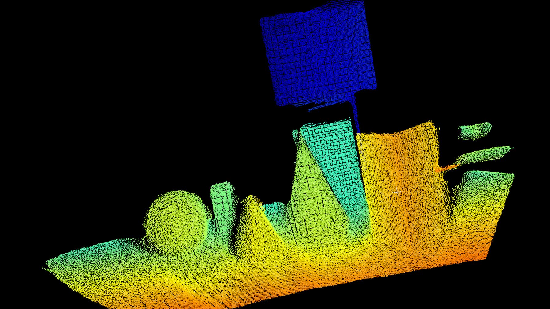
Well, “brief” may not be possible but here goes… The goal of both dToF and iTof is to create a depth map of a scene. This is not a 3D model, but a table of X-Y positions and the “open space” distance, or Z depth between the scanning system and the various objects in the scene.
Like a LiDAR point cloud?
Yes, a point cloud very similar to what a LiDAR sensor produces.
dToF works similarly to the parking sensors I mentioned before: a pulse of light is emitted from a laser at a known point in time and by recording the interval between this pulse and its reflection back from the target the round-trip distance can be calculated based on the speed of light. This is a point detection system, and as such the laser must be scanned across the scene. These systems typically use a special pixel type known as Single Photon Avalanche Diodes, or SPADs. These are used in groups to detect the laser pulse even at low intensities.
iToF uses a special pixel type and a laser but instead of the pixel being used to directly measure the time, it allows the measurement of the signal at a particular phase angle.
The technology behind this is a pixel called a Current-Assisted Photonic Demodulator, or CAPD. These pixels have the ability to store the collected signal during an exposure in one of two storage locations or “taps” – so one pixel – two taps. The selected tap is swapped at the same frequency as the laser light is modulated, with an additional control to delay the swap by a determined phase angle.
The two taps for each pixel can be read out separately. We do this several times – typically 4 – each with a different phase-angle delay. The phase difference between the outgoing laser and the returning light can then be calculated. It is then trivial to turn that measured phase into a distance travelled.
Right… “trivial”.
(laughter)
You mentioned the IMX570 DevKit just released by FRAMOS. How does it help iToF product development? What’s in the kit, and who is it intended for?
Yes indeed. FRAMOS has expanded its development module family to include Sony’s IMX570 sensor. An iToF system requires the synchronization of illumination and the sensor – as well as a processing pipe. These all work together to get good depth data per pixel. As such our target was to make sure everything is available and nothing “gets in the way”.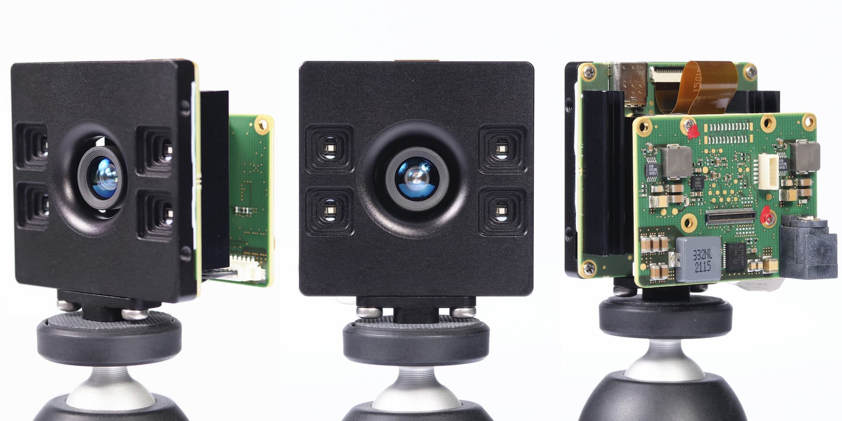
From a hardware perspective this means we have the sensor module with an aligned and glued lens and a separate illumination board with its dedicated power supply and connection to the sensor board.
Bolted to the back of the sensor board is a power and compute board. This compute board holds a SEP [Sensor Edge Processor], A.K.A a CXD5639. This device is able to convert the raw data input into calibrated depth and confidence data. We also added a small FPGA [Field-Programmable Gate Array] to facilitate the easy synchronization of this device with additional modules, including RGB modules.
The software and drivers are developed to provide quick and easy access to the SEP output and the RAW output from the sensor.
With the target development platform being the Jetson family from NVIDIA, (including Orin and Xavier), the devkit can be used by anyone looking to assess the iToF technology and develop a product around it. It’s helpful even if the final use case uses a different final compute platform.
The RAW data access, and fine control of the module operation provide great data for defining a final product and testing its capabilities. This includes using the key components in other system architectures that are outside the NVIDIA platforms – as well as the prototyping of a customized solution.
We’re talking about opportunities for customization of this kit. What sort of customization do you mean, and why would a user need to customize a development kit?
The devkit is a step on the road to building a product. It is a one-size-fits-all kit that focuses on flexibility. We can simulate many hardware and processing pipe configurations, enabling customers to build application layers, knowing that they can port that effort to their final products.
When transitioning to a production model, a customer’s application parameters will dominate the final design – much of which can be simulated with the devkit. From lens and illumination choices to PCB [Printed Circuit Board] size and shape.
Every application is different, including the environment, power budget accuracy, target behavior… the list can go on and on. We can offer the ability to tailor each and every component as well as providing an optimal configuration for the best price at the desired performance.
So what does customization mean in practical terms? What parts of this system can be changed, and how?
The Devkit is a belt-and-braces approach focusing on flexibility. When looking at solving a real world hardware requirement we would first look to reduce the bill of materials to support the minimum operational specification. The main target here is the number of laser emitters.
Next we would look at the consolidation of the components to a minimum size PCB, and one that is compatible with the customer’s target hardware such as heatsinking capability as well as the shape of the housing.
We would then select the components based on the optical requirements of the system. For example, changing the Field of View changes the lens, and therefore the lens mount. We also need to change the laser optic selection to provide the same Field of View as provided by the lens.
With this new hardware a new calibration may be requested, and this is solidly within the FRAMOS wheelhouse. So, not only can we build the device – we can generate a general calibration model as well as calibrating individual units as part of the production process.
The IMX570 sensor module and the Sensor Edge Processor both output data via the standard MIPI CSI-2 interface. There is no specific requirement to use the NVIDIA platform. Providing direct access to hardware otherwise controlled by the driver such as the laser drivers is a simple task, allowing the customer to completely build and control the acquisition of the iToF data when they are deploying or developing their IP [Intellectual Property] on any platform.
It is likely that any customized solution will need to interact with other hardware beyond simply using CSI-2. The removal or enhancement on the onboard timing FPGA, or providing CSI-2 data over GMSL spring to mind… But also customization includes other housekeeping capabilities, such as using the customer’s preferred bulk power solution. Using data/power connectors that can be preselected also allows for a more complete product efficiency.
You’ve mentioned working with a client to design or develop printed circuit boards, and other components of a camera system, but what about manufacturing them? Can FRAMOS be a manufacturing partner as well, and if so, what sort of volume can they produce?
Design must always be aware of the practicalities of manufacturing. In the case of iToF products this is particularly poignant, with the desire for an electrically and mechanically stable device that can hold its calibration during installation and operation. FRAMOS has the production capability both for lens active alignment and calibration. These capabilities are not just present for device quality improvements they also enable mass production to leverage savings at scale.
I appreciate your taking the time to sit down with me and talk about this. Do you have any closing thoughts?
Thank you too, I would like to mention that 3D data is now no longer just a gimmick, or for the metrology world. Adding 3D data to the arsenal of tools we have to solve problems is a fantastic opportunity to solve old and new problems alike. iToF and its interaction with the world is not a silver bullet. We need to consider many aspects of the application and technology to build good products with our customers. I, for one, am very excited to learn about what needs to be done and to help develop solutions to make it so.
Where could someone go to learn more about this development kit?
Good point, the kit can be found on the FRAMOS website at framos.com by simply looking for “Time-of-Flight”.